Week 6: Electronics Design
Wednesday 02/03/2016:
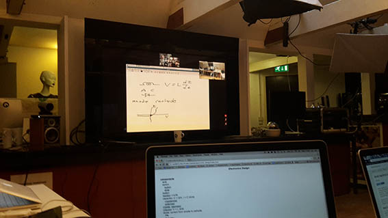
It was the first time that I really couldn’t follow Neil’s lecture at all. I was completely lost. My only hope was that I would somehow be able to gain some understanding during the week by breaking down the information and the deliverables to smaller steps.
Thursday 03/03/2016:
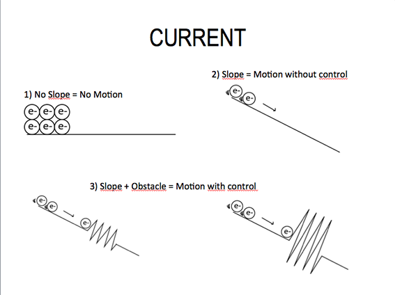
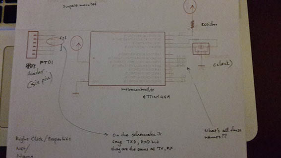
Emma started with a very clear and analytical lesson on circuits. I loved the examples in the images above which are taken from her lecture. Such examples, which create vivid images, are the best technique to transmit information to people who learn through the ‘visual learning style’, like myself.
At this point I feel that I need to describe some of the elements that we are using, as well as other terminology in order to get a better understanding of them. An obstacle for me is language; I sometimes need to recall the Greek words in order to remember what each component does. For purposes of better archiving for myself (and for future Fab Academy Greek speakers!) I am also providing the Greek words where useful/applicable. Most of the information below is taken from www.whatis.com and the chart from and the chart from allaboutcirquits here.
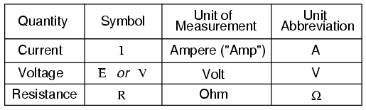
Current — ‘I’ (Ρεύμα): Current is a flow of electrical charge carriers, usually electrons or electron-deficient atoms.
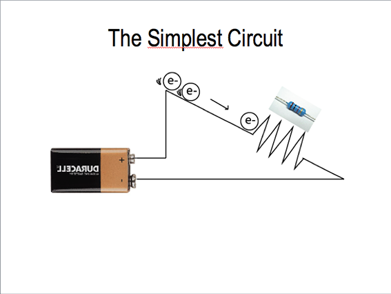

Volt/ Voltage — ‘V’ (Τάση): a quantitative expression of the potential difference in charge between two points in an electrical field, for example a battery. The greater the voltage, the greater the flow of electrical current.
Watt — ‘W’: It is used to specify the rate at which electrical energy is dissipated or the rate at which electromagnetic energy is radiated, absorbed, or dissipated.
Ampere — ‘A’: An ampere is a unit of measure of the rate of electro flow current in an electrical conductor.
Microcontroller (Μικροεπεξεργαστής): Microcomputer on a single chip.
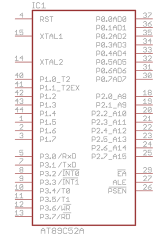
Capacitor (Πυκνωτής): A capacitor is a passive electronic component that stores energy in the form of an electrostatic field.

Resistor (Αντίσταση): A resistor is an electrical component that limits or regulates the flow of electrical current an electronic circuit. Resistors can also be used to provide a specific voltage for an active device such as a transistor.

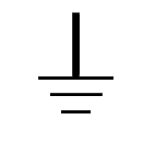
Ground (Γείωση): A ground is a direct electrical connection to the earth, a connection to a particular point in an electrical or electronic circuit.
Diode: A diode is a specialized electronic component with two electrodes called the anode and the cathode. The fundamental property of a diode is its tendency to conduct electric current in only one direction.

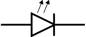
LED: A light-emitting diode (LED) is a semi-conductor device that emits visible light when an electric current passes through it. The light is not particularly bright, but in most LED's it is monochromatic, occurring at a single wavelength.
This is the battery symbol:

A useful thing to remember which will come in handy when having to calculate the components, to be put on a circuit, is the following equation: R=V/I or I= V/R or V=R*I
After carefully listening to the class, I felt quite proud that I followed it and I was ready to dive into this week’s exercise… If only.
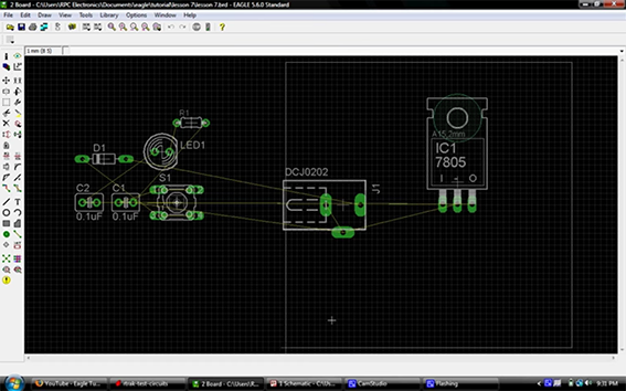
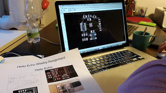
Instead I was faced with a new program: ‘CadSoft Eagle’ which I was not at all sure what it was supposed to do, or what I was supposed to do with it. Thankfully the whole class sat together to start the homework and I was able to realize that firstly, we had to draw up a ‘schematic’ diagram. Soon I understood that I was called to add the components of a circuit on this diagram, which is basically the representation of a circuit.
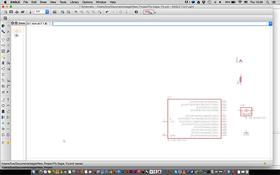
I downloaded and added the Fab Library to the Eagle Libraries list and I slowly started to add the components according to the official Fab Academy tutorial found here.
I added:
- a microcontroller
- an FTDI six pin connector
- an ISP header six pin connector
- a resonator
which are what comes standard on an Echo-Hello World board and proceeded to add:
- a switch
- and an LED
I was blindly following the tutorial up to that moment barely understanding what I was doing.
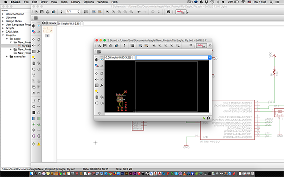
On Friday 04/03/2016: for some reason I hadn’t realized that we were sent links to Eagle CadSoft tutorials so I was feeling desperate to familiarize myself with the program while simultaneously feeling desperate to understand what was going on with the circuit! After finishing the schematic and still following the official tutorial it occurred to me that the shapes on the Eagle CadSoft ‘board’ view represented the elements and connections that I had made. I finally understood the purpose of using this program… Up to that point I just wanted to draw all the lines, boxes and circles in Illustrator and get this over with! This brought a feeling of relief because I was finally beginning to understand what Eagle CadSoft was doing. It also brought a feeling of panic because any mistakes I may have made in the schematic would cause problems in my final board…
Saturday 05/03/2016: I spent my day watching the Eagle CadSoft tutorials on this page and I understood that the lines that I was ‘routing’ represented the yellow lines (actually called ‘airwires’) connecting the components together. As I drew a route, the airwire disappeared which meant that the components were correctly connected together.
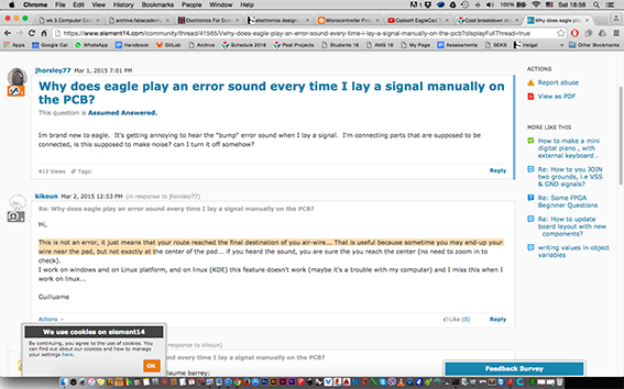
While routing, the airwires were changing places to suggest different valid connections, which was very useful when trying to avoid crossing lines and shorting the board. An important detail is that once a connection is made, a beep sounds to let us know that the route is successfully committed…
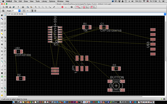
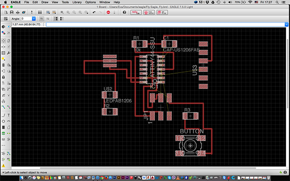
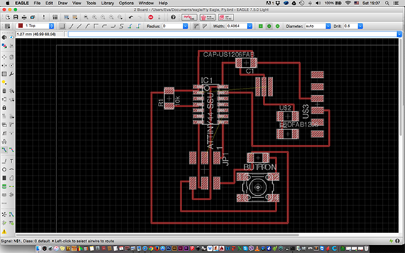
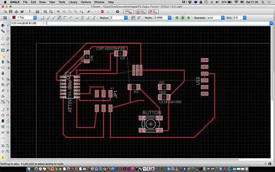
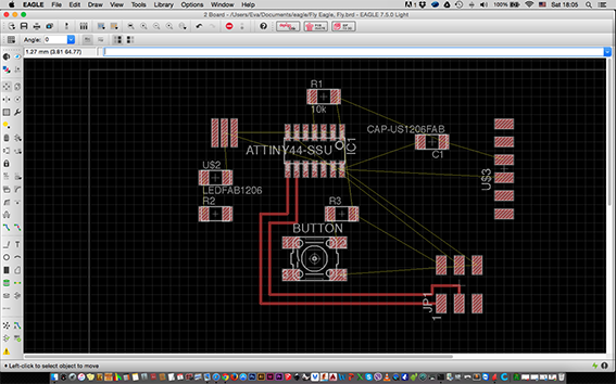
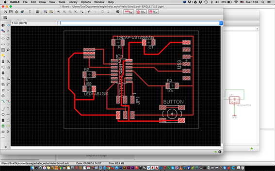
Sunday 06/03/2016: Since I finally understood what I was called to do, I proceeded to route my board, firstly by spacing out the components in order to get a clearer image of the traces I was called to complete. I attempted quite a few shapes. I set the route width to 0.40 after Emma’s suggestion. The plan was that if I had the time I would try to make a smaller board. I remained worried about whether I had done the schematic correctly because that would mean doing the routing all over again.
Monday 07/03/2016. Everything fell into place on Monday. Quite late in the process but I must admit I am actually getting interested in electronics after this week. Actually now that we have come to the end of this lesson I will watch Neil’s lecture again to see what has begun to make sense!
I went to the Fab Lab early to make sure that I would mill my board by the end of the day. Maybe I would even get to start stuffing it. I shared my progress with Emma and we carefully looked at the board and schematic together. At first, I thought that I was finished and would only need a 0Ohm capacitor to get over a shorting issue that I had come across. Emma pointed out that the ISP six-pin header had been wrongly connected and was shorting. I spent a lot of time re-arranging the elements and routes by looking at the board on the official Fab Tutorial and I realized that I was missing some connections. Firstly, my LED and switch were not part of the circuit but just floating around in the schematic! I added the wires with the ‘wire’ command, which of course made more airwires appear and needing to be routed without crossing. I thought of using the ‘auto route’ command but I opted not to, firstly because I wanted to go through the procedure myself. Another reason was that the command does not move the components around in order to make better connections. It just makes the connections from the positions on which they are already placed, so I realised that I would not have much control over the final outcome. It may also not complete all routing and the user may be left to do the donkey work anyway! I prefered to do it myself from the beginnning.
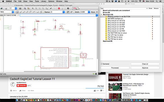
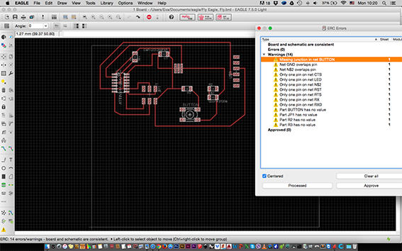
At that point Emma suggested going to The Eagle CadSoft menu/tools/erc to locate the errors. Thankfully I had no errors, the board and schematic were consistent, but I had 11 warnings!… These warnings meant nothing to me until Emma went through them with me, which helped me comprehend my mistakes. I understood that by giving the same name/label to a connection in the schematic, it means that it is actually connected. I also understood that by simply placing the switch and LED in the schematic did not mean that they were connected, but that I had to make the connections with the wire command myself. (It really doesn’t take a genius to figure this out, but I guess I really have dived into completely unknown territories!) Other warnings meant that there was an overlap in the wire and connection, while I thought the wire was snapping to the connection, the resistors needed values, and ‘missing junction’ means… missing dot on the schematic as junctions are represented with a dot.
To calculate the value of the resistors I had to apply Ohm’s Law which to me was a grey area. I didn’t know where to get the initial values in order to calculate the desired resistor value. Also to me the fact that 5mA is written as 0,005 was a revelation and so was that 1KΩ = 1000Ω!! This doesn’t take a genius either. Additionally, these values are measured with an ‘μ’, which is ‘m’ in Greek, but people refer to it as a ‘u’. At the same time ‘m’ is used for measuring ‘mili—’ This became even more confusing!
These values and representations of numbers are things that my brain refused to accept/comprehend/work with since school. I decided that I wasn’t going to need them in my life (and I have come this far without needing them!). My mind simply shuts down when it comes to numbers. I understand that I should get round to dealing with them if I want to make cool lights and that is the biggest reason I joined the Fab Academy. Is the objective of creativity and the production of cool products powerful enough to get me to understand electronics?
At some point I was finally able to calculate that I would need two 10k resistors and a 1k one. This brought up no more warnings and meant that I could proceed to milling my board. Piece of cake, right?
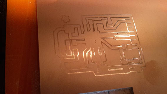
I firstly set up the Roland Modela and started to mill. I was pretty happy about my progress until Emma pranced by and said ‘it is not cutting’. This meant that the end-mill was not cutting through the copper although it was making a kind of trace and the fastest way to know this is that it does not produce any ‘sawdust’. I stopped it and I started again from the same position but adding a little more depth to it - 0,2 from 0,1. The offset was set to 4.
From then on it routed the… route just fine and I was getting excited about cutting all the way through. It is always exciting to get to hold what you had been working on the computer for a week. Unfortunately, when I ran the command to cut the outside trace, the mill ran over my routes and ruined my board… I had to start again.
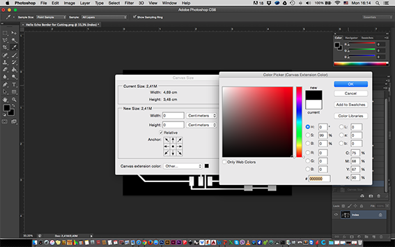
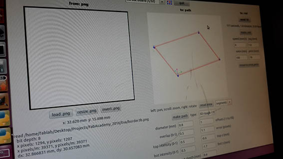
I thought that this probably meant that my border was not big enough so I returned to Photoshop to re-draw the border. I used the actual image of the route to extract the border from, exported as .png from Eagle, by changing the canvas size to 5mm larger than the image all around.
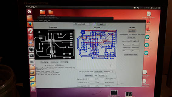
I proceeded to mill the paths again, with the offset set to 1 instead of 4, which was the setting for the first milling. This was done by mistake and probably because I was already stressing about time by then. The result was a much finer and much faster path and quite tidy. Since I had successfully routed those, I was ready to mill the outside border, starting from the same point from which I began to mill the path. And I milled over my paths again.
In my head it didn’t make sense that I had to start from the same coordinates as the paths, but having asked around me I understood that this was what I had to do. As it turns out, two things were going wrong. Firstly, I had not reversed the colors of the border. The Modella cuts the white and leaves the black colour. The endmill starts from the edge of the white shape and cuts inwards. So I returned to Photoshop and reversed the colours. The second mistake was that when the border is designed in Photoshop, one DOES NOT start to cut from the same co-ordinates but subtracts the border and adds the new position. If both paths and outside border are exported form the same Eagle CadSoft document this issue does not exist.
I tried to cut again, but the copper piece I had was a tight match to my PCB’s dimensions. In attempting to calculate my Photoshop made border, I placed the drawing too much to the inside of the copper plate, which did not leave enough room for the whole drawing to fit on it. By then I had to stop my hopeless efforts. Firstly, to allow my colleagues to cut and then to regroup myself, concentrate and do a correct mill.
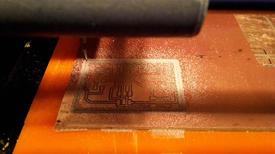
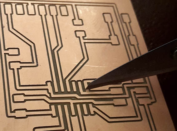
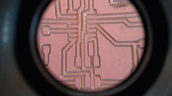
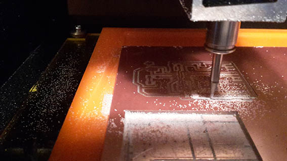
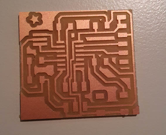
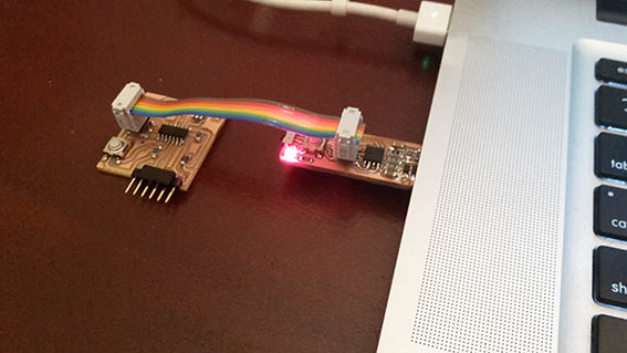
Tuesday 08/03/2016: Bright and early I followed Emma’s tutorial presentation on how to prepare the files for milling/ cutting which can be found here and proceeded to finally mill and cut my board. The cut was quite successful apart from a small area from which the Modela failed to remove the copper and it would create a shortage. I removed it with my scalpel. After seeing what happened with that minute detail, I will in the future use the multi-meter on the board before beginning to stuff. That way I will confirm that there will be no shortages or other unpleasant surprises of that sort.
The stuffing was pretty straightforward. I selected/ located my components more easily this time since I had better understanding at what I was doing and I proceeded to solder. The professional soldering iron with the fine tip is particularly useful and convenient to use since it allows for delicate handling of the zinc. It is important to first heat the copper spot onto which the component will go. Personally I add a little solder on one side of the component. I then attach and hold it in place for a few seconds to stabilize and then I add more zinc on the rest of the connections.
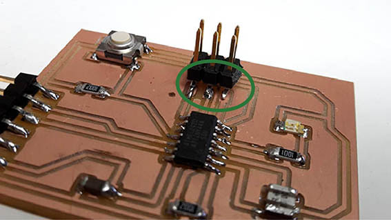
The tricky part was attaching the resonator, which needed to be touching on three separate paths. I attached its middle first and added solder on the four corners in order to connect its sides. I held the FTDI header in place with a piece of cardboard because it can’t stand on its own.
Another piece, which needed attention, was how to place the LED. The green line on the led needed to be located on the ground route. This can be located in two ways:
- Right clicking on routes in the board layout and selecting properties from the menu until the ground path is found.
- Pick the eye tool while in the schematic drawing and click on one of the ground symbols in it. This will reveal the ground route in the board drawing.
It seemed that everything was fine and that the board was ready. I started to verify my connections with the multi-meter. For the first time, I understood and was following my board paths, knew where I wanted the multi-meter to beep and where not to! Since everything was fine, I connected it to the ATTINY ISP. Care must be taken so that the two MISO pins are connected between them. I then typed ‘avrdude —c usbtiny —p t45’ in a terminal window to see if my board would be recognised. It wasn’t. I asked for the help of Emma who found the mistake but let me to locate it myself as usual (It’s more fun to be on the side of the teacher!). After careful inspection, I understood that I should also be checking my solder connections from the top of the connector pins rather than just their base. I had left a pin unsoldered so the connector was not working. This didn’t show in the multi-meter tests because I was touching it with the probes.
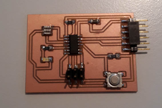
I added a little more solder and the ‘avrdude —c usbtiny —p t45’ command returned a ‘AVR device initialized and ready to accept instructions‘ message. Music to my ears.
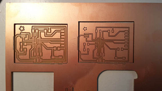
Since it was only lunch time I decided to stay at the Fab Lab and have a go at designing and cutting a smaller board. I purposely gave myself some space in the production of the first one just so I could be comfortable with routing and stuffing. (A couple of weeks later I realized that the above image means that the path connecting the pins of my FTDI header would be shorted. Please see Embedded Programming Week for the solution)
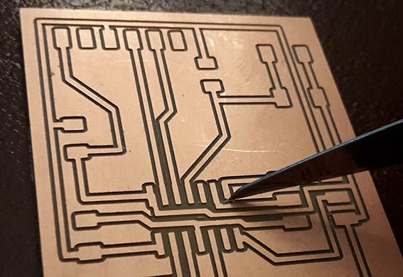
I did manage to finish and I milled the traces of the smaller PCB. It took me three efforts to cut around it, though. The Modella was only drilling holes on the board instead of cutting. At first it cut two at the back, so I re-exported form Eagle SoftCad. Then it drilled one on every corner. I went over the procedure again and I could see the trace in the fab modules but it was in red colour. The only parts which were blue were the corners. I sent the document to be cut again and it again drilled the same four holes. Emma to the rescue. As it turned out, my path was designed to a 0.4 mm width so I needed to give it a bigger diameter. The solution was found at 0.8mm and I did the cut.
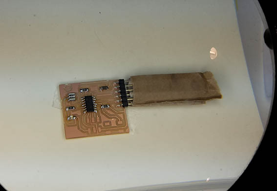
During stuffing, I used a small piece of cardboard in order to hold the FTDI in position while soldering. Another very useful trick that I learned from my colleague Jacopo Di Matteo is to put solder on all places where it should go. Then use the heat gun to heat them up and then gently place the element in place! Pretty useful for demanding pieces like microcontrollers.
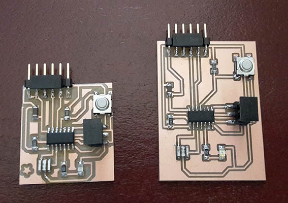
My smaller PCB board is now also stuffed and programmable!
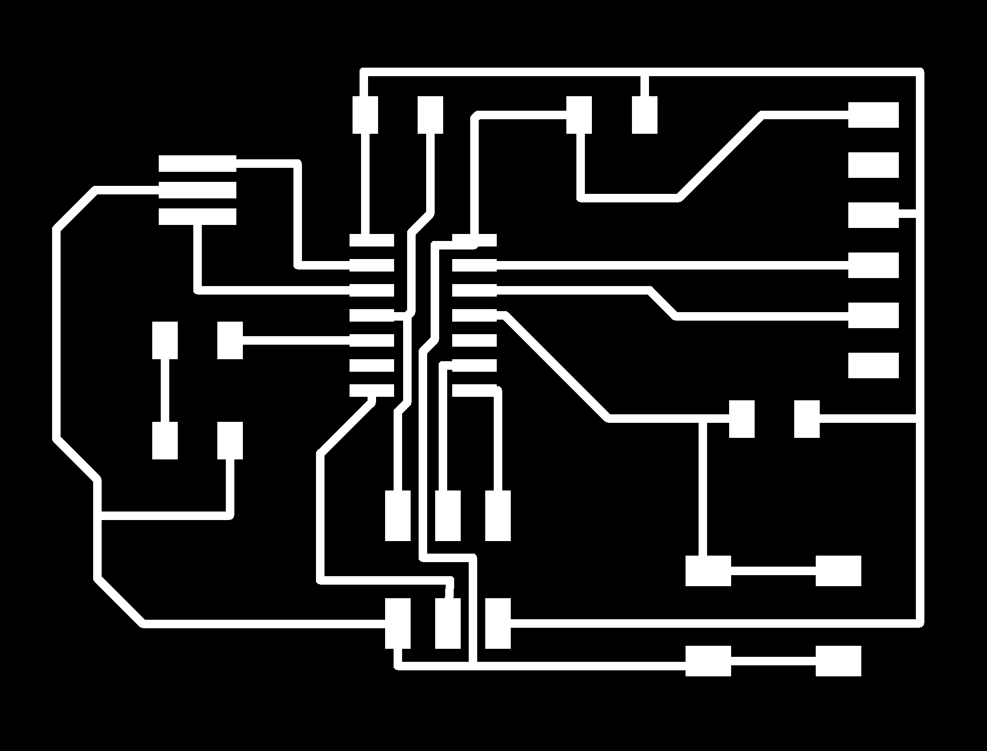
Hello Echo 1 SchematicHello Echo 1 Board
Hello Echo 1 Path
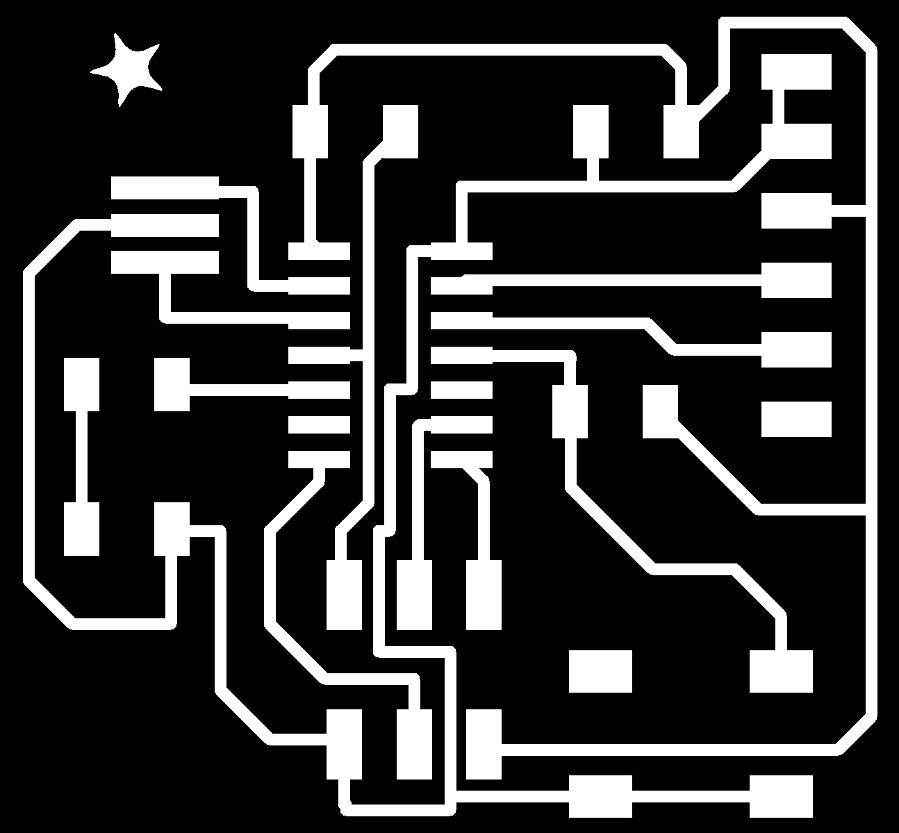
Hello Echo 1 Border Hello Echo 2 Schematic
Hello Echo 2 Board
Hello Echo 2 Path
Hello Echo 2 Border Electronics Design Lecture Back to Weekly Assignments Home